ClearStepsCLEARSTEPS AI
Teacher Login →Student Login →

Semiconductor Electronics: Class 12 Physics Practice Questions

18 original exam-pattern questions with full answers, matched to the current CBSE Class 12 paper design, including case-based questions. Attempt each question before opening the answer — or start a free 14-day trial ↓ for the full bank.

Q1Case-based4 marks

A student is building a simple DC power supply for a school project. She has four identical p-n junction diodes, a step-down transformer, and a capacitor. She connects the four diodes in a bridge configuration and places the capacitor across the output terminals to obtain a steady DC voltage from the 50 Hz AC mains supply.

A student is building a simple DC power supply for a school project. She has the following components available: four identical p-n junction diodes, a transformer (step-down), and a capacitor. She connects the four diodes in a bridge configuration followed by the capacitor across the output terminals.

(i) Name the type of rectifier circuit she has built. How many diodes conduct during the positive half-cycle of the AC input? (1 mark)

(ii) If the AC input frequency is 50 Hz, what is the frequency of the pulsating DC output before the capacitor is connected? Show your reasoning. (1 mark)

(iii) The student notices that after connecting the capacitor across the output, the voltage becomes much smoother. Explain the role of the capacitor in this circuit. (1 mark)

(iv) She replaces the bridge rectifier with only ONE diode (half-wave rectifier) but keeps the same 50 Hz input. What will be the output frequency now? Also state ONE disadvantage of the half-wave rectifier compared to the full-wave bridge rectifier. (1 mark)
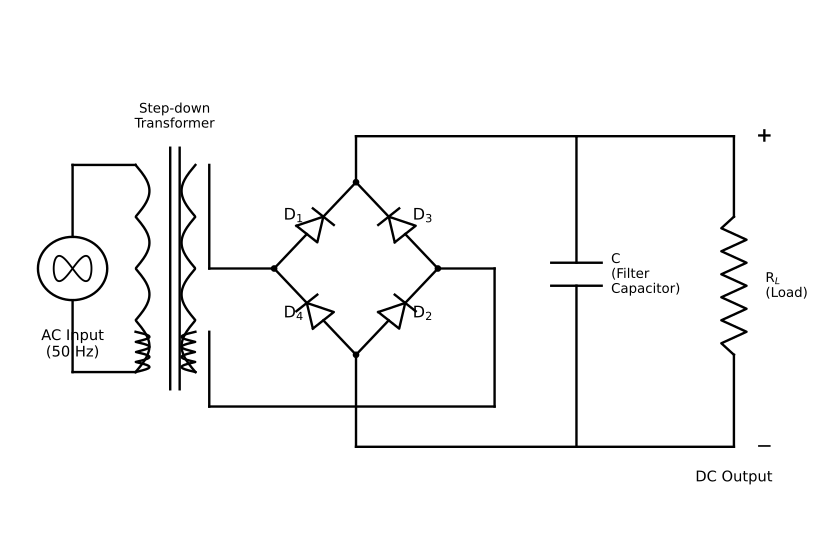
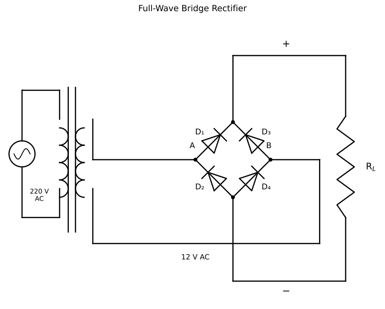
Diagram for question 1: Semiconductor Electronics
Show answer
(i) The circuit is a Full-Wave Bridge Rectifier.
During the positive half-cycle of the AC input, two diodes (out of the four) are forward-biased and conduct simultaneously, while the other two are reverse-biased.
∴ Number of diodes conducting in the positive half-cycle = 2.

(ii) In a full-wave rectifier, both the positive and negative half-cycles of the AC input are utilised. Each half-cycle of the input produces one pulse of output. Since there are two half-cycles per complete AC cycle:

f_out = 2 × f_input
→ f_out = 2 × 50 Hz
∴ Output frequency = 100 Hz.

(iii) The capacitor acts as a filter (smoothing capacitor).
During the rising part of each output pulse, the capacitor charges up to the peak voltage. During the falling part (when diode output drops), the capacitor discharges slowly through the load, maintaining the voltage at a nearly steady level. This charging and discharging action fills in the gaps between pulses, converting the pulsating DC into a smooth (almost constant) DC output.

(iv) In a half-wave rectifier, only one half-cycle (either positive or negative) is allowed to pass; the other is blocked by the single diode.

f_out = f_input = 50 Hz
∴ Output frequency = 50 Hz.

Disadvantage: The half-wave rectifier has greater ripple (less smooth output) compared to the full-wave bridge rectifier, because it utilises only one half of each AC cycle, resulting in larger gaps between successive output pulses and a lower average DC output voltage.
Q2Case-based4 marks

A solar cell manufacturing unit is testing two semiconductor wafers. Wafer X is doped with a pentavalent impurity (phosphorus) at a concentration of 10²¹ atoms/m³, and Wafer Y is doped with a trivalent impurity (boron) at the same concentration. The intrinsic carrier concentration nᵢ = 1.5 × 10¹⁶ m⁻³.

A solar cell manufacturing unit is testing two semiconductor wafers. Wafer X is doped with a pentavalent impurity (phosphorus) at a concentration of 10²¹ atoms/m³, and Wafer Y is doped with a trivalent impurity (boron) at the same concentration. The intrinsic carrier concentration nᵢ = 1.5 × 10¹⁶ m⁻³.

(i) Identify the type of semiconductor formed in each wafer and state the majority and minority carriers in each.

(ii) Calculate the minority carrier concentration in Wafer X.

(iii) When Wafers X and Y are used to form a p-n junction and forward biased, a depletion region exists at the junction. Explain, with reason, what happens to the width of the depletion region as the forward bias voltage is gradually increased.

(iv) The same p-n junction is now reverse biased. A technician observes that beyond a certain reverse voltage, a large current suddenly flows. Name this phenomenon and state ONE condition necessary for it to occur.

Show answer
(i) Wafer X is doped with phosphorus (Group V / pentavalent), so it is an n-type semiconductor. Majority carriers: electrons; Minority carriers: holes.
Wafer Y is doped with boron (Group III / trivalent), so it is a p-type semiconductor. Majority carriers: holes; Minority carriers: electrons.
[1 mark]

(ii) By the mass-action law: nₑ · nₕ = nᵢ²
In Wafer X (n-type), the majority carrier (electron) concentration nₑ ≈ Nₐ = 10²¹ m⁻³ (since doping >> nᵢ).
∴ nₕ = nᵢ² / nₑ = (1.5 × 10¹⁶)² / 10²¹
= (2.25 × 10³²) / 10²¹
∴ Minority carrier (hole) concentration in Wafer X = 2.25 × 10¹¹ m⁻³
[1 mark]

(iii) In forward bias, the external voltage opposes the built-in potential barrier across the depletion region. As the forward bias voltage is gradually increased, the electric field due to the external source opposes the internal electric field of the depletion region. This causes majority carriers (electrons from n-side and holes from p-side) to drift towards the junction and recombine, thereby reducing the uncompensated ion layer on both sides.
∴ The width of the depletion region decreases as forward bias voltage is increased.
[1 mark]

(iv) The phenomenon observed is Zener breakdown (or avalanche breakdown, depending on doping and junction design; for heavily doped junctions it is Zener breakdown).
Condition necessary: The reverse bias voltage must reach or exceed the breakdown voltage (Zener voltage, Vz) of the junction. At this voltage, the electric field across the depletion region becomes strong enough to break covalent bonds directly (Zener mechanism) or accelerate carriers to cause ionisation by collision (avalanche mechanism), producing a large reverse current.
[1 mark]
Q3Case-based4 marks

A student is setting up a simple LED-based indicator circuit for a school science project. She has a red LED (silicon-based p-n junction), a 9 V battery, and a 470 Ω resistor. She notices that when she connects the LED directly to the battery without the resistor, the LED glows very brightly for a moment and then stops working permanently. However, when she connects the 470 Ω resistor in series with the LED, it glows steadily.

A student is setting up a simple LED-based indicator circuit for a school science project. She has a red LED (silicon-based p-n junction), a 9 V battery, and a 470 Ω resistor. She notices that when she connects the LED directly to the battery without the resistor, the LED glows very brightly for a moment and then stops working permanently. However, when she connects the 470 Ω resistor in series with the LED, it glows steadily.

(i) Identify the type of biasing (forward or reverse) required for the LED to emit light. Name the majority carriers that cross the junction under this condition in a p-type and n-type region respectively.

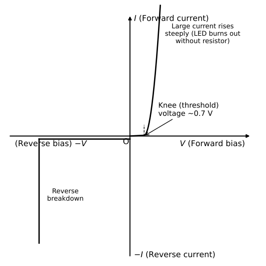
(ii) Explain why connecting the LED directly to the 9 V battery (without the resistor) caused it to burn out. Use the V–I characteristic of a p-n junction diode to support your answer.

(iii) The forward voltage drop across the LED is 2 V. Calculate the current flowing through the LED when the 470 Ω resistor is connected in series with the 9 V battery.

(iv) The student accidentally reverses the connections of the LED in the circuit (with the 470 Ω resistor still present). Will the LED glow? Give one reason for your answer.

Diagram for question 3: Semiconductor Electronics
Show answer
(i) Forward biasing is required for the LED to emit light.
Under forward bias, the p-side is connected to the positive terminal and the n-side to the negative terminal of the battery. The majority carriers crossing the junction are:
• p-type region: holes (move towards the junction)
• n-type region: electrons (move towards the junction)
When these majority carriers recombine at the junction, energy is released as photons (light). ✓

(ii) The V–I characteristic of a p-n junction diode in forward bias shows that beyond the threshold (knee) voltage (~0.7 V for silicon), the current rises very steeply with a very small increase in voltage — the forward resistance becomes extremely small.
When the LED is connected directly to 9 V (well beyond the knee voltage) without any current-limiting resistor, the forward current becomes extremely large (theoretically limited only by the tiny internal resistance of the battery and junction). This very large current causes excessive power dissipation (P = I²R) inside the junction, generating heat that permanently damages (burns out) the semiconductor material. ✓
The resistor acts as a current-limiting element, keeping the current in the safe operating range.

(iii) By Kirchhoff's Voltage Law (KVL) applied to the series circuit:
V_battery = V_LED + V_resistor
∴ V_resistor = V_battery − V_LED

Substituting values:
V_resistor = 9 V − 2 V = 7 V

Using Ohm's Law: I = V_resistor / R
I = 7 V / 470 Ω

∴ I ≈ 0.0149 A ≈ 14.9 mA ✓

(iv) No, the LED will NOT glow.
Reason: When the LED connections are reversed, it is under reverse bias. Under reverse bias, the depletion region widens and the potential barrier increases, allowing only a negligibly small reverse saturation current (of the order of microamperes) to flow — far too small to cause any carrier recombination or light emission. ✓
Q4Case-based4 marks

A electronics student is working on a project to build a DC power supply. She uses a transformer to step down 220 V AC mains supply to 12 V AC. She then connects four identical p-n junction diodes in a bridge arrangement (full-wave bridge rectifier) to convert AC to pulsating DC. The output of the rectifier is connected across a load resistor R_L. The student observes that the output frequency is twice the input frequency. She also notes that during the positive half-cycle, diodes D₁ and D₃ conduct, while during the negative half-cycle, diodes D₂ and D₄ conduct. She then uses a filter capacitor to smooth the output.

Read the following passage and answer the questions that follow:

A electronics student is working on a project to build a DC power supply. She uses a transformer to step down 220 V AC mains supply to 12 V AC. She then connects four identical p-n junction diodes in a bridge arrangement (full-wave bridge rectifier) to convert AC to pulsating DC. The output of the rectifier is connected across a load resistor R_L. The student observes that the output frequency is twice the input frequency. She also notes that during the positive half-cycle, diodes D₁ and D₃ conduct, while during the negative half-cycle, diodes D₂ and D₄ conduct. She then uses a filter capacitor to smooth the output.

(i) Name the process by which an extrinsic semiconductor is obtained from a pure semiconductor. If silicon is doped with phosphorus (Group V), what type of semiconductor is formed and what are the majority charge carriers?

(ii) In a p-n junction diode, what is the direction of the built-in electric field in the depletion region? How does forward biasing affect the width of the depletion region?

(iii) The student measures the input AC frequency as 50 Hz. What is the frequency of the pulsating DC output from the full-wave bridge rectifier? Justify your answer.

(iv) The student replaces the bridge rectifier with a single diode (half-wave rectifier) using the same 50 Hz input. Compare the output frequency and the efficiency of rectification of a half-wave rectifier with that of the full-wave bridge rectifier used earlier. (Answer in one or two sentences each.)

Diagram for question 4: Semiconductor Electronics
Show answer
(i) The process of adding a small amount of suitable impurity (pentavalent or trivalent) to a pure (intrinsic) semiconductor to increase its conductivity is called doping.

When silicon (Group IV) is doped with phosphorus (Group V, pentavalent impurity), an n-type semiconductor is formed.

In an n-type semiconductor, electrons are the majority charge carriers and holes are the minority charge carriers.

∴ Type formed: n-type; Majority carriers: electrons.

(ii) In a p-n junction, the built-in electric field in the depletion region is directed from the n-side to the p-side (i.e., from the positive donor ion-cores on the n-side toward the negative acceptor ion-cores on the p-side).

Effect of forward biasing: When a p-n junction is forward biased, an external voltage is applied that opposes the built-in electric field. This reduces the potential barrier, and as a result, the width of the depletion region decreases.

∴ Built-in field: n-side → p-side; Forward bias → depletion width decreases.

(iii) By the relation for a full-wave rectifier:

f_out = 2 × f_in

Substituting: f_out = 2 × 50 Hz

∴ f_out = 100 Hz

Justification: In a full-wave bridge rectifier, both the positive and the negative half-cycles of the input AC are utilised. Each complete input cycle produces two output pulses (one from D₁, D₃ during the positive half-cycle and one from D₂, D₄ during the negative half-cycle), so the output frequency is twice the input frequency.

(iv) Comparison between half-wave rectifier and full-wave bridge rectifier:

| Parameter | Half-Wave Rectifier | Full-Wave Bridge Rectifier |
|---|---|---|
| Output frequency | Equal to input frequency: f_out = 50 Hz | Twice the input frequency: f_out = 100 Hz |
| Rectification efficiency | Lower (~40.6%) — only one half-cycle is used | Higher (~81.2%) — both half-cycles are used |

∴ The half-wave rectifier has lower output frequency (50 Hz) and lower rectification efficiency compared to the full-wave bridge rectifier (100 Hz output frequency, approximately double the efficiency).
Q5Case-based4 marks

A student sets up a circuit for a school science project. She connects a silicon p-n junction diode in forward bias with a 9 V battery and a series resistor of 820 Ω. The threshold (knee) voltage of the silicon diode is 0.7 V. In forward bias, the voltage across the conducting diode equals its threshold voltage, and the remaining voltage drops across the series resistor.

A student sets up a simple circuit to power an LED indicator light in a school science project. She connects a silicon p-n junction diode in forward bias with a 9 V battery and a series resistor of 820 Ω. The threshold (knee) voltage of the silicon diode is 0.7 V.

(i) What is the voltage dropped across the series resistor when the diode is conducting?
(ii) Calculate the current flowing through the circuit.
(iii) The student now reverses the battery terminals. Explain what happens to the current through the circuit and why.
(iv) She replaces the silicon diode with a germanium diode (threshold voltage 0.3 V), keeping all other components the same (9 V battery, 820 Ω resistor). Will the current through the circuit increase, decrease, or remain the same compared to part (ii)? Justify your answer with a calculation.

Show answer
(i) Voltage across the series resistor:

By Kirchhoff's Voltage Law (KVL), the sum of voltage drops around the loop equals the EMF of the battery.

∴ V_R = V_battery − V_diode

→ V_R = 9 V − 0.7 V

∴ V_R = 8.3 V

(ii) Current through the circuit:

By Ohm's Law, V = IR, so I = V_R / R

→ I = 8.3 V / 820 Ω

∴ I = 0.0101 A ≈ 10.1 mA

(iii) Effect of reversing battery terminals:

When the battery terminals are reversed, the diode is connected in reverse bias. In reverse bias, the depletion region widens and the potential barrier across the p-n junction increases, opposing the flow of majority carriers. As a result, practically no current (only a negligibly small reverse saturation current of the order of μA) flows through the circuit. For all practical purposes, the current through the circuit is zero.

(iv) Comparison with germanium diode (threshold voltage = 0.3 V):

For the germanium diode:

V_R(Ge) = V_battery − V_diode(Ge) = 9 V − 0.3 V = 8.7 V

I(Ge) = V_R(Ge) / R = 8.7 V / 820 Ω

∴ I(Ge) ≈ 10.6 mA

Since 10.6 mA > 10.1 mA, the current increases when the germanium diode is used. This is because the germanium diode has a lower threshold voltage (0.3 V vs 0.7 V), so a greater voltage is available across the series resistor, resulting in a higher current.
Q6MCQ1 mark

In an n-type semiconductor, which of the following correctly identifies the majority and minority charge carriers?

Show answer
Option (B) is correct.

Explanation: In an n-type semiconductor, a pentavalent (Group V) donor impurity (e.g., Arsenic or Phosphorus) is added to the pure semiconductor. Each donor atom contributes one free electron to the conduction band. Therefore, electrons are the majority charge carriers and holes are the minority charge carriers.
Q7Short Answer1 mark

Assertion (A): A p-type semiconductor has holes as majority carriers and electrons as minority carriers.
Reason (R): When a trivalent impurity (acceptor) is doped into an intrinsic semiconductor, it creates holes in the valence band, making holes more numerous than thermally generated electrons.

Show answer
Option (a) is correct.

Explanation: In a p-type semiconductor, a trivalent (Group III) impurity such as boron is added to an intrinsic semiconductor. Each acceptor atom has only three valence electrons and creates one hole in the valence band by accepting an electron. This greatly increases the hole concentration, making holes the majority carriers and thermally generated electrons the minority carriers (n<sub>e</sub> · n<sub>h</sub> = n<sub>i</sub><sup>2</sup>). Therefore, Assertion (A) is true. Reason (R) correctly and completely explains the physical mechanism behind Assertion (A). ∴ Both (A) and (R) are true, and (R) is the correct explanation of (A).
Q8MCQ1 mark

In an n-type semiconductor, which of the following are the majority charge carriers?

Show answer
Option (C) is correct.

Explanation: In an n-type semiconductor, a pentavalent (Group V) impurity (donor) is added to a pure semiconductor such as Si or Ge. The donor atom donates one extra electron to the conduction band. Therefore, electrons are the majority charge carriers in an n-type semiconductor (holes are the minority carriers).
Q9MCQ1 mark

In a p-n junction diode, the depletion region is formed due to:

Show answer
Option (B) is correct.

Explanation: When a p-n junction is formed, holes (majority carriers in p-region) diffuse into the n-region and electrons (majority carriers in n-region) diffuse into the p-region due to the concentration gradient across the junction. These diffusing majority carriers recombine near the junction, leaving behind immobile ionised donor and acceptor atoms. This region, depleted of free charge carriers, is called the depletion region. It is thus the diffusion of majority carriers — not drift, minority carrier flow, or any external field — that is responsible for the formation of the depletion region.
Q10Short Answer2 marks

What is meant by the 'depletion region' in a p-n junction diode? State how its width changes when the diode is (i) forward biased and (ii) reverse biased.

Show answer
The depletion region is the narrow region formed on either side of the p-n junction from which mobile charge carriers (electrons and holes) have diffused away and recombined, leaving behind immobile ionised donor and acceptor atoms. It acts as a potential barrier (~0.6 V for Si) opposing further diffusion of carriers.

(i) Forward bias: The external voltage opposes the built-in potential barrier, so majority carriers are pushed towards the junction. ∴ The depletion region becomes narrower.

(ii) Reverse bias: The external voltage adds to the built-in potential barrier, pulling majority carriers away from the junction. ∴ The depletion region becomes wider.
Q11Short Answer2 marks

Why does the width of the depletion region in a p-n junction decrease when it is forward biased? Explain briefly.

Show answer
In a p-n junction, the depletion region is formed due to the diffusion of majority carriers across the junction, creating a built-in electric field (barrier potential) directed from the n-side to the p-side.

When the junction is forward biased, the positive terminal of the battery is connected to the p-side and the negative terminal to the n-side. The applied electric field opposes the built-in electric field of the junction.

∴ This reduces the net electric field across the depletion region, causing majority carriers (holes from p-side and electrons from n-side) to drift back towards the junction, neutralising some of the immobile ions. As a result, the width of the depletion region decreases.
Q12Short Answer2 marks

In an extrinsic semiconductor, the number density of electrons is 2 × 10¹⁹ m⁻³ and the intrinsic carrier concentration is 1.5 × 10¹⁶ m⁻³. What type of semiconductor is it, and what is the number density of holes in it?

Show answer
By the mass-action law for an extrinsic semiconductor:

n<sub>e</sub> · n<sub>h</sub> = n<sub>i</sub><sup>2</sup>

Since n<sub>e</sub> = 2 × 10<sup>19</sup> m<sup>⁻³</sup> >> n<sub>i</sub> = 1.5 × 10<sup>16</sup> m<sup>⁻³</sup>, electrons are the majority carriers.

∴ The semiconductor is n-type. (½ mark)

Substituting:

n<sub>h</sub> = n<sub>i</sub><sup>2</sup> / n<sub>e</sub> = (1.5 × 10<sup>16</sup>)<sup>2</sup> / (2 × 10<sup>19</sup>)

n<sub>h</sub> = (2.25 × 10<sup>32</sup>) / (2 × 10<sup>19</sup>)

∴ n<sub>h</sub> = 1.125 × 10<sup>13</sup> m<sup>⁻³</sup> (½ mark)
Q13Short Answer3 marks

A pure germanium semiconductor has an intrinsic carrier concentration nᵢ = 2.4 × 10¹⁹ m⁻³. It is doped with indium (a trivalent impurity) at a concentration of 4.8 × 10²³ atoms per m³.
(a) Identify the type of semiconductor formed and name the majority and minority carriers.
(b) Calculate the concentration of majority carriers and minority carriers in the doped germanium.

Show answer
Part (a): [1 mark]

Indium belongs to Group III (trivalent impurity). When added to germanium, each indium atom creates an electron-vacancy (hole), acting as an acceptor impurity.
∴ The semiconductor formed is a p-type semiconductor.
Majority carriers: holes
Minority carriers: electrons

Part (b): [2 marks]

By the law of mass action for an extrinsic semiconductor:

nₑ · nₕ = nᵢ²

For a p-type semiconductor, when the dopant concentration Nₐ >> nᵢ, the majority carrier (hole) concentration is approximately equal to the acceptor concentration:

nₕ ≈ Nₐ = 4.8 × 10²³ m⁻³

∴ Majority carrier concentration, nₕ = 4.8 × 10²³ m⁻³

Now, applying the mass action law to find minority carrier (electron) concentration:

nₑ = nᵢ² / nₕ

nₑ = (2.4 × 10¹⁹)² / (4.8 × 10²³)

nₑ = (5.76 × 10³⁸) / (4.8 × 10²³)

∴ Minority carrier concentration, nₑ = 1.2 × 10¹⁵ m⁻³
Q14Short Answer3 marks

A semiconductor device manufacturer is designing a temperature sensor using an intrinsic silicon wafer. At room temperature (300 K), the intrinsic carrier concentration of silicon is nᵢ = 1.5 × 10¹⁶ m⁻³. To improve conductivity at room temperature, the wafer is doped with phosphorus (a Group V element) at a concentration of ND = 4.5 × 10²¹ m⁻³.

(a) Identify the type of semiconductor formed after doping and name the majority and minority carriers. (1 mark)

(b) Calculate the majority carrier (electron) concentration nₑ and the minority carrier (hole) concentration nₕ in the doped semiconductor. (2 marks)

(c) The engineer observes that when the doped semiconductor is heated to a very high temperature, it begins to behave like an intrinsic semiconductor again. Give ONE reason for this observation. (1 mark)

Show answer
(a) Since phosphorus belongs to Group V (pentavalent impurity), it donates one extra electron to the silicon lattice. The semiconductor formed is n-type semiconductor.

Majority carriers: electrons
Minority carriers: holes

[1 mark]

(b) By the law of mass action for an extrinsic semiconductor:

nₑ · nₕ = nᵢ²

Since the doping concentration ND >> nᵢ, the majority carrier concentration equals the donor concentration:

nₑ ≈ ND = 4.5 × 10²¹ m⁻³

Applying the mass-action law to find minority carrier concentration:

nₕ = nᵢ² / nₑ

nₕ = (1.5 × 10¹⁶)² / (4.5 × 10²¹)

nₕ = (2.25 × 10³²) / (4.5 × 10²¹)

∴ nₑ = 4.5 × 10²¹ m⁻³ and nₕ = 5 × 10¹⁰ m⁻³

[2 marks: 1 for correct formula and nₑ; 1 for correct substitution and ∴ nₕ with unit]

(c) At very high temperatures, a large number of covalent bonds in the silicon lattice break due to thermal energy, generating a very large number of electron–hole pairs. The thermally generated intrinsic carriers (nᵢ) far outnumber the donor-contributed electrons, so the contribution of the dopant becomes negligible compared to the intrinsic carrier concentration. As a result, nₑ ≈ nₕ ≈ nᵢ and the semiconductor effectively behaves like an intrinsic semiconductor.

[1 mark]
Q15Short Answer3 marks

A student is designing a solar-powered street light. She uses a silicon p-n junction photodiode connected in reverse bias to detect ambient light levels. During the day, when light falls on the junction, the reverse current increases significantly. At night, with no light, the reverse current drops to a very small value (dark current).

(i) Why is the photodiode operated in reverse bias rather than forward bias for light detection?
(ii) When light of frequency ν falls on the photodiode, what is the minimum condition (in terms of the energy band gap E_g of silicon) for electron-hole pair generation?
(iii) The student observes that when the light intensity doubles, the photocurrent also approximately doubles, but the dark current remains nearly unchanged. Identify the physical origin of (a) the photocurrent and (b) the dark current.
(iv) Silicon (E_g ≈ 1.1 eV) is preferred over germanium (E_g ≈ 0.7 eV) for this outdoor photodiode application. Give ONE reason why.

Show answer
(i) In reverse bias, the depletion region widens and the reverse saturation current is very small in the dark. When photons of sufficient energy strike the junction, they generate electron-hole pairs in or near the depletion region. The strong built-in electric field (augmented by the reverse bias) immediately sweeps these minority carriers across the junction — electrons to the n-side and holes to the p-side — producing a measurable photocurrent proportional to light intensity. In forward bias, the large forward current (majority carrier current) would completely swamp the much smaller photo-generated minority carrier signal, making light detection impractical.

(ii) By Planck's quantum condition, a photon can create an electron-hole pair only if its energy equals or exceeds the energy band gap of the material.

∴ Condition: hν ≥ E_g

where h = 6.63 × 10⁻³⁴ J s and E_g is the band gap of silicon (≈ 1.1 eV ≈ 1.76 × 10⁻¹⁹ J).

Equivalently, the threshold (minimum) frequency is ν₀ = E_g / h.

(iii)
(a) Photocurrent: When photons with hν ≥ E_g strike the depletion region, they excite valence-band electrons into the conduction band, generating electron-hole pairs (minority carriers). The reverse-bias field sweeps electrons toward the n-side and holes toward the p-side, constituting the photocurrent. Since each photon generates one pair, doubling intensity doubles the number of photons per second and hence doubles the photocurrent.

(b) Dark current: Even without illumination, thermal agitation at room temperature continuously generates a small number of electron-hole pairs within the depletion and diffusion regions. The minority carriers so produced are swept across by the electric field, giving a small temperature-dependent reverse saturation (dark) current. It is independent of light intensity and changes only with temperature.

(iv) Silicon (E_g ≈ 1.1 eV) has a larger band gap than germanium (E_g ≈ 0.7 eV). Therefore, at room temperature (and especially on warm sunny days outdoors), thermally generated electron-hole pairs are far fewer in silicon than in germanium. This means silicon has a significantly smaller dark current, resulting in a higher signal-to-noise ratio and more reliable light detection in outdoor conditions.
Q16Short Answer3 marks

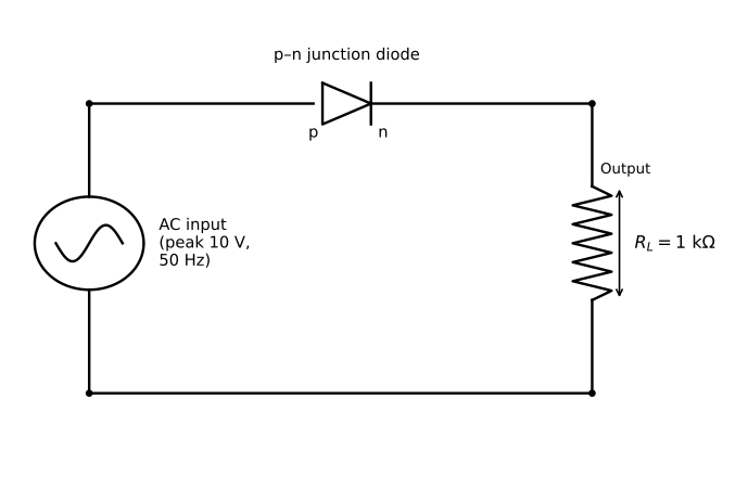
A student in a physics laboratory connects a p-n junction diode made of silicon in a circuit to test its rectifying action. She applies an alternating voltage of peak value 10 V and frequency 50 Hz across the diode in series with a load resistance R_L = 1 kΩ. She observes that current flows through R_L only during one half of each cycle.

(i) Name the type of rectifier circuit described above and state how many diodes are used in it.
(ii) What is the output frequency of the rectified signal across R_L?
(iii) During the half-cycle when current flows, the diode conducts. Explain why current does NOT flow during the other half-cycle, with reference to the depletion region of the diode.
(iv) If the student replaces the single diode with a bridge rectifier (four diodes), state ONE advantage she would observe in the output waveform.

Diagram for question 16: Semiconductor Electronics
Show answer
(i) The circuit described is a Half-Wave Rectifier. It uses ONE (1) diode.

(ii) In a half-wave rectifier, only one half of each input cycle appears at the output.
∴ Output frequency = Input frequency = 50 Hz.

(iii) During the conducting half-cycle, the p-n junction is forward biased — the p-side is at higher potential than the n-side. The external voltage reduces the width of the depletion region and lowers the potential barrier (~0.6 V for Si), allowing majority carriers to cross and current to flow.

During the other half-cycle, the junction is reverse biased — the n-side is at higher potential. The external voltage widens the depletion region and increases the potential barrier. Majority carriers cannot cross this barrier, so effectively no current flows through R_L (only a negligible reverse saturation current due to minority carriers exists).

(iv) Advantage of a bridge (full-wave) rectifier: Current flows through R_L during BOTH half-cycles of the input. The output frequency doubles to 100 Hz, giving a smoother (less fluctuating) DC output with smaller ripple, making it more efficient than the half-wave rectifier.
Q17Short Answer3 marks

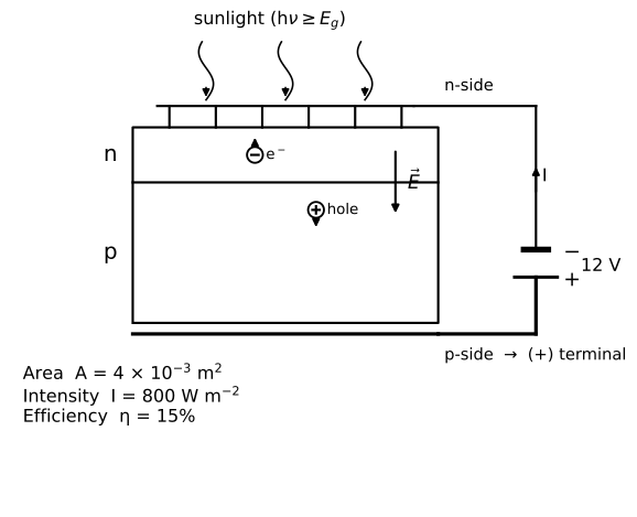
A solar-powered street-light system uses a silicon p-n junction solar cell to charge a 12 V battery during the day. The solar cell has an area of 4 × 10⁻³ m² and is illuminated by sunlight of intensity 800 W m⁻². The cell has an efficiency of 15%.

(i) Name the three basic processes involved in the generation of emf by a solar cell and briefly explain each.
(ii) The p-side of the solar cell is connected to the positive terminal of the battery. A student claims this is incorrect because in a p-n junction under forward bias, conventional current flows from n to p inside the junction. Analyse whether the student's claim is correct or incorrect, giving a reason based on how a solar cell operates.
(iii) Calculate the electrical power output of the solar cell.
(iv) If the solar cell charges the 12 V battery, calculate the charging current delivered to the battery. (Assume the cell operates at its calculated output power.)

Diagram for question 17: Semiconductor Electronics
Show answer
(i) The three basic processes in a solar cell are:

(1) Generation: When photons of incident sunlight (with energy hν ≥ E<sub>g</sub>, where E<sub>g</sub> ≈ 1.1 eV for silicon) are absorbed near the p-n junction, electron–hole pairs (EHPs) are generated.

(2) Separation: The built-in electric field E⃗ across the depletion region (directed from n-side to p-side) sweeps the photo-generated electrons toward the n-side and holes toward the p-side, separating the charge carriers before they can recombine.

(3) Collection: The separated electrons accumulate on the n-side and holes on the p-side. When an external circuit is connected, electrons flow out through the n-terminal, do work in the circuit, and return through the p-terminal — constituting a current. This builds up the photovoltaic emf.

(ii) The student's claim is INCORRECT.

A solar cell does not operate under externally applied forward bias; it acts as a source of emf (like a battery). The built-in field of the depletion region drives photo-generated holes to the p-side and electrons to the n-side. ∴ The p-side acquires a higher potential (positive terminal) and the n-side acquires a lower potential (negative terminal). Conventional current flows from the p-terminal through the external circuit — exactly as the student's connection shows. The solar cell is self-biased by light; the direction of current is opposite to that in a forward-biased diode used as a rectifier.

(iii) By definition, efficiency η is given by:

η = P<sub>out</sub> / P<sub>in</sub>

First, calculate incident power:
P<sub>in</sub> = Intensity × Area = 800 × 4 × 10<sup>−3</sup> = 3.2 W

η = 15% = 0.15

P<sub>out</sub> = η × P<sub>in</sub> = 0.15 × 3.2

∴ P<sub>out</sub> = 0.48 W

(iv) Using P = V × I, where V = 12 V (battery terminal voltage) and P = P<sub>out</sub> = 0.48 W:

I = P / V = 0.48 / 12

∴ Charging current I = 0.04 A (= 40 mA)
Q18Short Answer3 marks

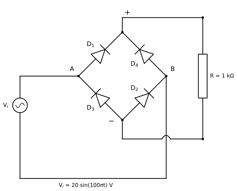
A student builds a full-wave bridge rectifier circuit using four identical silicon diodes (each with a forward voltage drop of 0.7 V) and connects it to a pure resistive load R = 1 kΩ. The input is an ac signal V_i = 20 sin(100πt) V.

(i) During the positive half-cycle, identify which two diodes (label them D₁, D₂, D₃, D₄ in the standard bridge arrangement) conduct and briefly justify.
(ii) Calculate the peak output voltage across the load R.
(iii) Calculate the average (dc) output voltage across the load R.
(iv) If the load resistance is now doubled to 2 kΩ (keeping the same input), state with reason whether the average output voltage increases, decreases, or remains the same.

Diagram for question 18: Semiconductor Electronics
Show answer
(i) In the standard bridge rectifier, the four diodes are arranged so that during the positive half-cycle, current flows through the path: A → D₁ → R (load) → D₂ → B.
Therefore, diodes D₁ and D₂ conduct during the positive half-cycle.
Justification: D₁ and D₂ are forward-biased (anode at higher potential than cathode) during this half-cycle, while D₃ and D₄ are reverse-biased and hence do not conduct. [1 mark]

(ii) The peak output voltage across the load is obtained by subtracting the voltage drops across the two conducting diodes from the peak input voltage.

Formula: V_peak(output) = V_peak(input) − 2 × V_f

where V_peak(input) = 20 V and V_f = 0.7 V (forward drop per diode).

Substituting:
V_peak(output) = 20 − 2 × 0.7
V_peak(output) = 20 − 1.4

∴ V_peak(output) = 18.6 V [1 mark]

(iii) For a full-wave rectifier, the average (dc) output voltage is related to the peak output voltage by:

Formula: V_avg = 2 V_peak(output) / π

Substituting:
V_avg = (2 × 18.6) / π
V_avg = 37.2 / 3.14

∴ V_avg ≈ 11.85 V ≈ 11.8 V [1 mark]

(iv) The average output voltage remains the same.

Reason: The average (dc) output voltage of a full-wave bridge rectifier is given by V_avg = 2V_peak(output)/π, which depends only on the peak input voltage and the forward voltage drops of the diodes — not on the value of the load resistance R. Since the input voltage and diode parameters are unchanged, doubling R does not alter V_avg. (However, the average load current I_avg = V_avg/R will decrease by half.) [1 mark]

Want unlimited practice on Semiconductor Electronics?

The full ClearSteps bank has 18+ reviewed questions on this chapter alone — with step-wise solutions, difficulty levels, and progress tracking. Verify your WhatsApp number and your free trial starts right here.

CBSE · CLASS 12
🎟️14-day free trial · code PRAC auto-applied
Mobile Number
+91
OTP will be sent to your WhatsApp

⭐ Trusted by 12,000+ students across India

Semiconductor Electronics Class 12 Physics Questions